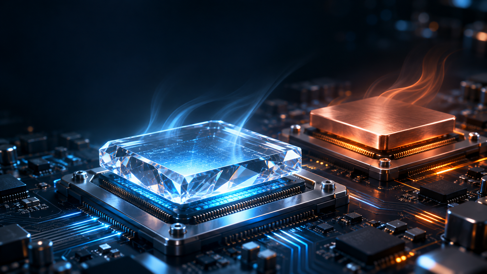
On November 5, 2026, Diamond Foundry announced it had grown a 200-millimeter single-crystal diamond, the same diameter as a standard semiconductor wafer, and pitched it as a heat spreader for AI chips. The sample was shown as-grown and unpolished, and the company did not publish thickness, defect density, yield, or cost data (Diamond Foundry; Hardware Busters).
That gap between the announcement and the missing numbers is the whole story. Single-crystal diamond conducts heat better than any practical engineering material, roughly five times better than copper, and AI accelerators are increasingly limited by how fast heat can escape a few square millimeters of silicon. The physics is not in dispute. What remains unproven is whether anyone can grow, slice, polish, and bond diamond onto chips with the uniformity, yield, reliability, and price that semiconductor manufacturing demands. The evidence as it stands points to a split answer: diamond cooling in general is crossing from the lab into early commercial servers, but the single-crystal version at full wafer scale is still a materials milestone waiting for its manufacturing proof.
Why diamond embarrasses copper on paper

Heat in a chip is carried by lattice vibrations called phonons. Diamond's stiff carbon bonds and light atoms let phonons travel with very little scattering, which is why high-quality single-crystal diamond reaches a room-temperature thermal conductivity of roughly 2,000 to 2,200 W/m·K (MPCVD diamond thin films study). Copper, the default heat-spreader material in electronics, sits around 380 to 450 W/m·K, while commercial CVD diamond grades span roughly 700 to 2,200 W/m·K depending on quality (Element Six CVD Diamond Handbook).
Diamond has a second advantage copper cannot match: it is electrically insulating. A spreader can sit directly against or even surround active circuitry without shorting anything, which opens integration options, such as diamond interposers and diamond layers deposited inside the package, that are impossible with metal.
The catch is that a chip is not a block of one material. It is a stack of silicon, metals, solders, adhesives, and substrates, and heat must cross every boundary in that stack. A spreader that is superb in isolation can be throttled by the glue that attaches it.
What happens when diamond meets real chips
The strongest independent device evidence so far comes from gallium nitride (GaN) power transistors, which concentrate extreme heat at tiny gate regions. A peer-reviewed IEEE study wrapped GaN high-electron-mobility transistors in a 500-nanometer "all-around" diamond layer and measured gate temperatures 98 ± 19 °C lower than control devices at 9.5 W/mm of DC power. The result held across multiple devices and wafer locations and was cross-checked with three independent thermometry methods, making it far stronger than a simulation claim (IEEE Xplore). Notably, that demonstration, like most device-level results in the 2023 to 2024 literature, used polycrystalline CVD diamond, not single-crystal.

Packaging-level results point the same direction. A 2024 IEEE study found a diamond interposer in a 2.5D package (where multiple chiplets sit side by side on a connecting substrate) cut peak temperature by 23.9 °C and thermal resistance by 0.75 °C/W compared with a silicon interposer, though this measured package-level heat removal rather than an exposed transistor hotspot (IEEE Xplore). Separate 2.5D-chiplet experiments with an integrated diamond spreader reported more than 20 °C lower peak temperature and thermal impedance near 0.023 °C/W (ScienceDirect). For silicon processors specifically, a 2024 report claimed microcrystalline CVD diamond raised junction-to-case thermal conductance by 84 percent and lowered junction temperature by roughly 20 °C under measured workloads (ResearchGate).
There is now early commercial evidence too. Akash Systems announced servers built around AMD Instinct MI350X GPUs with diamond bonded at the GPU, manufactured by MiTAC and described as deployed products under existing AMD and OEM warranties. The company claims up to 10 °C lower GPU temperature, 22 percent higher FLOPs per watt, 15 percent higher throughput in hot ambient conditions, and up to 100 percent lower cooling power (Akash Systems). Those figures are company-reported results from Akash's own testing, not independently published benchmarks, so they should be read as configuration-specific claims rather than general improvements for all AI chips (Akash Systems). Even so, warranted, OEM-manufactured servers represent a meaningful step past laboratory demonstration.
Element Six, the industrial diamond arm of De Beers, has shown a diamond spreader in a laboratory silicon test assembly handling hot-spot loads up to 100 W at roughly 9.3 kW/cm², though in a controlled test structure rather than a production accelerator (Element Six case study).
The interfaces can eat the advantage

Before heat reaches the diamond, it must cross a bonding layer, and that crossing is where diamond's advantage leaks away. Thermal engineers measure this with thermal boundary conductance: how readily heat jumps across the junction between two materials. An IEEE Electronics Packaging Society analysis notes that interface resistance can dominate the total thermal resistance of a diamond-cooled stack, meaning a perfect diamond layer behind a poor bond loses much of its advantage (IEEE EPS).
Researchers are attacking the bond itself. Room-temperature surface-activated bonding of silicon carbide to diamond, followed by annealing, has produced thermal-boundary conductance near 93 MW·m⁻²·K⁻¹, with further gains attributed to converting the amorphous silicon bonding layer into silicon carbide (Functional Diamond). Direct die-to-wafer bonding of thin single-crystal diamond films offers another route that could parallelize large-area assembly, but interface cleanliness, alignment, voids, and bond strength remain central yield challenges (arXiv).
An alternative is to skip bonding entirely and grow diamond directly on finished chips. Microwave-plasma CVD has produced 200 to 300-nanometer films with conductivity above 300 W/m·K at substrate temperatures near 450 °C, low enough to be compatible with back-end chip processing. But low-temperature growth tends to create small grains, non-diamond carbon, pinholes, and slow deposition, all of which cut conductivity and threaten economic throughput (ScienceDirect). Note the number: 300 W/m·K is below copper. Deposited diamond at chip-friendly temperatures currently sacrifices most of the material's headline advantage.
Where this story sits
5 related pieces
Read it →
Hover a story · click to read
 No. 24 · Sep 2, 2026Whole Servers, Hidden Compute: Taiwan and the New AI Export Problem
 No. 45 · Sep 12, 2026China's Supply Chain Chokepoints: What De-Risking Costs, and Whether It Works
 No. 58 · Oct 3, 2026A Foundry of One's Own: What a TSMC-Run Terafab Would Mean for Musk's Companies, Intel, and US Chip Self-Sufficiency
 No. 41 · Sep 7, 2026Stress-Testing the American Empire: Real Decline or Cyclical Strain?
 No. 35 · Sep 5, 2026China's quiet rare-earth chokepoint on U.S. defense and chip supply chains
Why single-crystal diamond resists manufacturing
Everything above mostly used polycrystalline diamond, which is easier to make but scatters phonons at its grain boundaries. Single-crystal diamond is where the 2,200 W/m·K figure lives, and it is where manufacturing gets genuinely hard.
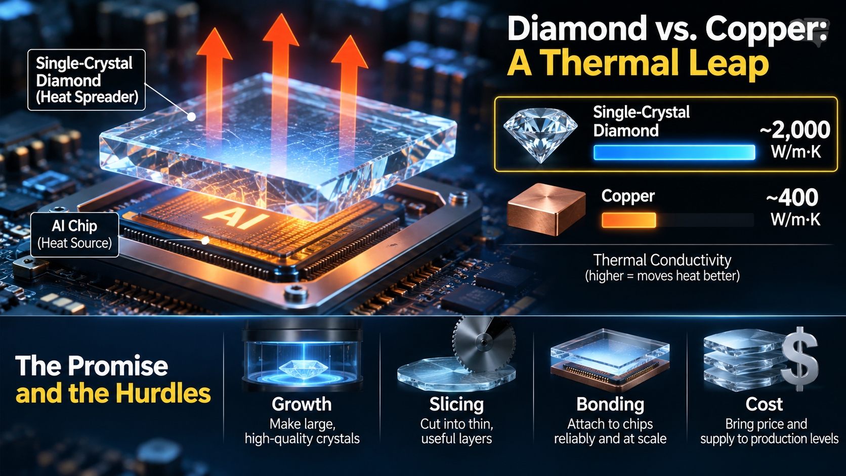
Growing single crystals large enough matters first. Repeated growth cycles can enlarge a crystal, but edge polycrystal formation, seed degradation, and repeated process interruptions hurt throughput and repeatability. Mosaic growth, which tiles small seed crystals and grows them together into one plate, is more practical for inch-scale substrates, but misalignment, gaps, twins, voids, and defects at the coalescence boundaries create fracture and device-yield risks (Functional Diamond review). Three-dimensional facet growth has reached roughly 100 μm/h in millimeter-scale crystals, yet quality progressively deteriorates as growth spreads across multiple facets (Functional Diamond).
Then the crystal must be cut and flattened, and diamond's defining property works against it. Its hardness causes rapid tool wear, subsurface damage, warpage, and cracking, with conventional slicing kerf losses reported at roughly 20 to 50 percent, meaning up to half the grown material can be ground away as waste. Candidate slicing methods include fixed-abrasive diamond wire, nanosecond-to-femtosecond lasers, and wire electrical-discharge machining for conductive diamond. Reported substrate costs can reach several hundred to several thousand dollars per square centimeter, reflecting low material utilization, long processing times, specialized tooling, and scrap from breakage (Functional Diamond review). For scale: an AI accelerator die is several square centimeters, and such GPUs ship in high volume.
This is why Diamond Foundry's 200-mm crystal, impressive as a growth achievement, does not yet answer the manufacturing question. Public reporting identifies the missing data plainly: thickness, defect density, growth time, yield, finished-wafer cost, and verified chip-level thermal performance (Hardware Busters; Tom's Hardware).
Does diamond physically fit inside a chip package?
Mostly, yes, and in one respect better than copper. CVD diamond's coefficient of thermal expansion is roughly 1.5 to 1.8 ppm/K, close to silicon's, which means a diamond layer bonded to a silicon die expands and contracts almost in step with it as the chip heats and cools (Nature Communications Engineering). Copper's much larger expansion mismatch against silicon is a known source of stress; it is part of why interface design matters so much in copper-based cooling (MDPI review).

But a package also contains metals, solders, and organic substrates whose expansion is far larger than diamond's. The IEEE EPS analysis warns that this mismatch can generate wafer bow, cracking, delamination, and cycling-induced interface degradation (IEEE EPS). Diamond solves one stress problem at the silicon face and creates another at the package face.
Will it survive years of heating, cooling, and vibration?
AI chips cycle between idle and full power thousands of times, and every cycle flexes every interface in the stack. Here the evidence is thin, and what exists is cautionary. In one reliability study of a silver-diamond composite spreader, specimens survived ten room-temperature-to-350 °C cycles followed by 500 cycles or shocks between −55 °C and 125 °C, but testing still found reduced thermal conductivity, increased effective expansion, and structural changes at the silver-diamond interface afterward (Journal of Microelectronics and Electronic Packaging). That was a composite, not a bonded single-crystal plate, so it does not directly condemn single-crystal integration, but it shows diamond-metal interfaces degrading under exactly the stresses a server imposes.
Vibration compounds the risk. Packaging research identifies temperature, humidity, vibration, and dust as major stressors, and combined thermal and vibratory loading can accelerate fatigue at bonds and interfaces (Frontiers in Electronics). Multi-year power-cycling data for single-crystal diamond bonded to a production AI accelerator does not appear to have been published. That absence is not evidence of failure, but it is exactly the data a chipmaker would demand before qualification.
Who pays, and who controls the supply?

Diamond does not need to beat copper on price per gram. It needs to earn back its premium somewhere else in the system. An analysis published by Diamond Foundry argues the economic case is strongest where hotspot suppression raises allowable power, reliability, or lifetime enough to offset the spreader cost, reporting potential permissible-power gains of 2.1× to 5.0× as package-side heat transfer improves (Diamond Foundry). If a diamond layer lets a data center run the same GPU at meaningfully higher sustained power, or cuts cooling energy as Akash claims for its configuration, the spreader premium can disappear into total cost of ownership. If it only shaves a few degrees off a chip that was not thermally limited, it never pays.
Supply is the other constraint. Market analysis indicates fewer than ten firms control most diamond thermal-spreader capacity, with Chinese producers expanding lower-cost polycrystalline grades (IndexBox). That concentration cuts both ways: a focused supplier like Element Six or Diamond Foundry could scale quickly for a committed customer, but there is no sign yet of a competitive, qualified, multi-vendor supply chain for single-crystal diamond wafers comparable to the one chipmakers rely on for silicon.
Meanwhile copper is not standing still. It is cheap, machinable, and supply-chain mature, and the industry is compensating for its lower conductivity with better interface materials, thinner stacks, and liquid-cooling architectures co-designed with the chip layout (MDPI review). Diamond has to beat not today's copper solution but the copper-plus-liquid-cooling solution of three years from now.
What would move diamond from milestone to production line?
The evidence suggests a clear checklist. Pilot production of single-crystal diamond cooling would be justified when a supplier can publicly demonstrate, in roughly this order: polished wafers at 100 mm or larger with characterized defect density and thickness uniformity; a bonding process with thermal boundary conductance high enough that the interface no longer dominates the stack; measured junction-temperature reduction on a production-class accelerator, verified by an independent lab; power-cycling and vibration data over qualification-length test campaigns; and a finished cost per die that the permissible-power gain actually repays.
Today, polycrystalline CVD diamond has cleared several of those bars at device level, and diamond-cooled servers are shipping in at least one warranted commercial configuration, albeit with vendor-reported performance numbers (Akash Systems). Single-crystal diamond has cleared only the first fraction of the first bar. The 200-mm crystal proves the material can be grown at wafer diameter; it proves nothing yet about slicing it without losing half the material, polishing it to bonding-grade flatness, attaching it without voids, or doing all of that at a yield and price a foundry would accept.

So the honest answer to the opening question is conditional. Diamond cooling for AI chips is no longer just a laboratory curiosity; it is already in pilot commercial use. Single-crystal diamond, the version that fully delivers the material's legendary conductivity, remains a laboratory milestone, and the barriers keeping it there are not physics. They are kerf losses, defect densities, bond yields, cycling data, and dollars per square centimeter, which is to say they are exactly the kind of problems the semiconductor industry has spent sixty years learning to grind down, when the payoff justifies the grind.
Sources / References
- Diamond Foundry, "D200mm: A New Scale for Single-Crystal Diamond," November 2026. https://www.df.com/insights/d200mm-single-crystal-diamond
- Hardware Busters, "Diamond Foundry Grows a 200mm Single-Crystal Diamond and Pitches It as an AI Chip Heat Spreader." https://hwbusters.com/news/diamond-foundry-grows-a-200mm-single-crystal-diamond-and-pitches-it-as-an-ai-chip-heat-spreader/
- Tom's Hardware, "Diamond Foundry creates world's first 200mm single-crystal diamond wafer." https://www.tomshardware.com/pc-components/cooling/diamond-foundry-creates-worlds-first-200mm-single-crystal-diamond-wafer-massive-gem-aims-to-solve-ai-chip-cooling-crisis-envisioned-as-a-cooling-material-for-semiconductors
- "MPCVD diamond thin films as heat spreaders for back end of the line (BEOL) silicon chip fabrication," ScienceDirect. https://www.sciencedirect.com/science/article/pii/S0925963525010568
- "Novel all-around diamond integration with GaN HEMTs demonstrating highly efficient device cooling," IEEE Conference Publication. https://ieeexplore.ieee.org/document/10019509/
- "Investigation of Heat Dissipation and Electrical Properties of Diamond Interposer for 2.5-D Packagings," IEEE Journals & Magazine, 2024. https://ieeexplore.ieee.org/document/10614611/
- "High-efficient and fast-response thermal management by heterogeneous integration of diamond on interposer-based 2.5D chiplets," ScienceDirect. https://www.sciencedirect.com/science/article/pii/S2451904926003161
- "Performance Envelope Enabled by CVD Diamond Heatspreader Integration in Semiconductor Chips," 2024. https://www.researchgate.net/publication/377227170_Performance_envelope_enabled_by_CVD_diamond_heatspreader_integration_in_semiconductor_chips
- Akash Systems, "Akash Systems Announces World's First Diamond Cooled AI Servers with AMD Instinct MI350X GPUs and MiTAC Computing." https://akashsystems.com/post/akash-systems-announces-worlds-first-diamond-cooled-ai-servers-with-amd-instinct-tm-mi350x-gpus-and-mitac-computing
- Akash Systems, "Artificial Intelligence." https://www.akashsystems.com/industries/artificial-intelligence
- Element Six, "The CVD Diamond Handbook." https://e6cvd.com/media/wysiwyg/pdf/CVD_Diamond_Handbook_digital_01.07.20.pdf
- Element Six, "Diamond heat spreader case study." https://e6-prd-cdn-01.azureedge.net/mediacontainer/medialibraries/element6/documents/brochures/diamond-heat-spreader-case-study.pdf?ext=.pdf
- IEEE Electronics Packaging Society, "Diamond Thermal Interface" analysis. https://eps.ieee.org/wp-content/uploads/2026/02/EDMS_Diamond_Thermal_Interface.pdf
- "Fabrication of low thermal resistance 3C-SiC/diamond structure for GaN epitaxial layer growth," Functional Diamond. https://www.tandfonline.com/doi/pdf/10.1080/26941112.2024.2337352
- "Advances and challenges in single crystal diamond growth via microwave plasma chemical vapor deposition," Functional Diamond, 2026. https://doi.org/10.1080/26941112.2026.2669069
- "Growing and polishing methods aiming at CVD diamond wafer over 10-inch," Functional Diamond, 2025. https://doi.org/10.1080/26941112.2025.2523762
- "Die to wafer direct bonding of (100) single-crystal diamond thin films for quantum optoelectronics," arXiv. https://arxiv.org/abs/2603.17140
- "Thermal management of 3-D heterogeneously integrated microelectronics: challenges and future research directions," Communications Engineering (Nature). https://www.nature.com/articles/s44172-026-00590-y
- "Reliability Assessment of a New Power Electronics Packaging Material: Silver Diamond Composite," Journal of Microelectronics and Electronic Packaging. https://imapsjmep.org/article/39850-reliability-assessment-of-a-new-power-electronics-packaging-material-silver-diamond-composite
- "Electronics packaging materials and component-level degradation monitoring," Frontiers in Electronics. https://www.frontiersin.org/journals/electronics/articles/10.3389/felec.2025.1506112/full
- "Thermal Management Challenges in 2.5D and 3D Chiplet Integration: A Review on Architecture–Cooling Co-Design," MDPI Eng. https://www.mdpi.com/2673-4117/6/12/373
- Diamond Foundry, "Adding Cooling Capacity to SCD Substrates: Microchannels, etc." https://www.df.com/insights/cooling-scd-substrates
- IndexBox, "Diamond Thermal Spreader Substrates Market in the World." https://www.indexbox.io/store/world-diamond-thermal-spreader-substrates-market-analysis-forecast-size-trends-and-insights/
The reading behind this research
What the desk leaned on for this piece. Each link goes to the retailer, where the price is shown.

Arctic Silver Ceramique 2 2.7g Premium High Density Thermal Cooling Compound Retail (CMQ2-2.7G)
The article notes a spreader can be throttled by the glue attaching it; this paste is the home-PC version of that heat-transfer layer.
View on Walmart
The article notes a great spreader can be throttled by the glue attaching it; this paste is that interface layer between a PC's chip and its cooler.
View on Walmart
Thermalright Odyssey Thermal Pad
The article says heat must cross every layer in a chip stack and a weak interface can throttle even diamond; this is that interface layer.
View on Walmart
HV-F2056 Laptop Cooling Pad for 15.6-17 Inch Laptops, Black
The article notes AI chips are limited by how fast heat escapes; a laptop faces the same problem at home, and this pad helps air move under it.
View on Walmart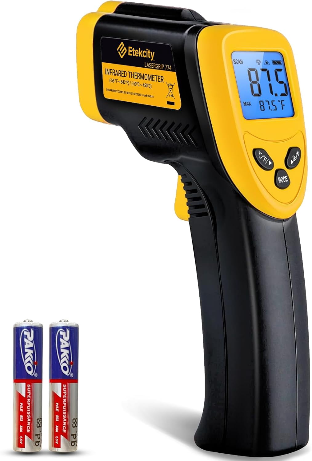
Infrared Thermometer Laser Temperature Gun 774
The article measures diamond cooling in degrees shaved off chip heat; this lets you check surface temperatures on your own laptop or GPU.
View on Walmart
The Diamond Makers Paperback Edition
Tells the history of how lab-grown diamond became possible, background for the article's question of growing 200 mm single-crystal wafers.
View on WalmartPaid links. Calibre Code USA may earn a commission from purchases made through these links. This does not affect what we write or what we recommend.
Comments (2)
Continue exploring
A Foundry of One's Own: What a TSMC-Run Terafab Would Mean for Musk's Companies, Intel, and US Chip Self-Sufficiency
Musk's October 3, 2026 confirmation of TSMC-Terafab talks raises a question the chip industry has never had to answer: what…
Stress-Testing the American Empire: Real Decline or Cyclical Strain?
Interest costs, gold hoarding and allied rearmament say decline; chips, energy and capital markets say resilience. Here is the…
China's quiet rare-earth chokepoint on U.S. defense and chip supply chains
Chinese rare-earth exporters are reportedly refusing U.S. orders even where licenses exist. Inside the licensing, sanctions, and…
I worked with diamond-bonded accelerator prototypes, and the claimed 10 °C GPU reduction did not appear in our rack measurements. The package ran cooler at the spreader, but hotspot temperatures and system-level cooling power were essentially unchanged, so the Akash figures should not be treated as representative of deployed AI servers.
The practical bottleneck is the interface, not the 2,000–2,200 W/m·K headline conductivity. Before treating a 200 mm wafer as manufacturing-ready, vendors need to show bond-line thickness, thermal-boundary resistance, warpage, and reliability after repeated thermal cycling; otherwise the adhesive or solder can erase much of the diamond’s advantage.